Low-voltage amplifier using transistors. The simplest low-frequency amplifiers using transistors. Cascade ULF circuits using bipolar transistors
The transistor amplifier, despite its long history, remains a favorite subject of research for both beginners and seasoned radio amateurs. And this is understandable. It is an indispensable component of the most popular low (sound) frequency amplifiers. We will look at how simple transistor amplifiers are built.
Amplifier frequency response
In any television or radio receiver, in every music center or sound amplifier you can find transistor sound amplifiers (low frequency - LF). The difference between transistor audio amplifiers and other types lies in their frequency characteristics.
A transistor-based audio amplifier has a uniform frequency response in the frequency band from 15 Hz to 20 kHz. This means that the amplifier converts (amplify) all input signals with a frequency within this range approximately equally. The figure below shows the ideal frequency response curve for an audio amplifier in the coordinates “amplifier gain Ku - input signal frequency.”
This curve is almost flat from 15 Hz to 20 kHz. This means that such an amplifier should be used specifically for input signals with frequencies between 15 Hz and 20 kHz. For input signals with frequencies above 20 kHz or below 15 Hz, its efficiency and performance degrade quickly.
The type of frequency response of the amplifier is determined by the electrical radio elements (ERE) of its circuit, and primarily by the transistors themselves. A transistor-based audio amplifier is usually assembled using so-called low- and mid-frequency transistors with a total input signal bandwidth from tens and hundreds of Hz to 30 kHz.
Amplifier operating class
As is known, depending on the degree of continuity of current flow throughout its period through a transistor amplification stage (amplifier), the following classes of its operation are distinguished: “A”, “B”, “AB”, “C”, “D”.
In operating class, current “A” flows through the cascade for 100% of the input signal period. The operation of the cascade in this class is illustrated by the following figure.

In the operating class of the amplifier stage "AB", current flows through it for more than 50%, but less than 100% of the input signal period (see figure below).

In the "B" stage operation class, the current flows through it for exactly 50% of the input signal period, as illustrated in the figure.

Finally, in class C stage operation, current flows through it for less than 50% of the input signal period.
Low-frequency amplifier using transistors: distortion in the main classes of operation
In the working area, a class “A” transistor amplifier has a low level of nonlinear distortion. But if the signal has pulsed voltage surges, leading to saturation of the transistors, then higher harmonics (up to the 11th) appear around each “standard” harmonic of the output signal. This causes the phenomenon of so-called transistor, or metallic, sound.
If low-frequency power amplifiers using transistors have an unstabilized power supply, then their output signals are amplitude modulated near the mains frequency. This leads to a harsh sound at the left end of the frequency response. Various methods of voltage stabilization make the amplifier design more complex.
The typical efficiency of a single-ended class A amplifier does not exceed 20% due to the constantly open transistor and the continuous flow of a constant current component. You can make a class A amplifier push-pull, the efficiency will increase slightly, but the half-waves of the signal will become more asymmetrical. Transferring a cascade from operating class “A” to operating class “AB” quadruples nonlinear distortions, although the efficiency of its circuit increases.
In class “AB” and “B” amplifiers, distortion increases as the signal level decreases. One involuntarily wants to turn up such an amplifier louder to fully experience the power and dynamics of the music, but often this does not help much.
Intermediate grades of work
Work class "A" has a variation - class "A+". In this case, the low-voltage input transistors of an amplifier of this class operate in class “A”, and the high-voltage output transistors of the amplifier, when their input signals exceed a certain level, go into classes “B” or “AB”. The efficiency of such cascades is better than in pure class “A”, and nonlinear distortions are less (up to 0.003%). However, they also have a “metallic” sound due to the presence of higher harmonics in the output signal.
In amplifiers of another class - "AA" the degree of nonlinear distortion is even lower - about 0.0005%, but higher harmonics are also present.
Return to the Class A transistor amplifier?
Today, many experts in the field of high-quality sound reproduction advocate a return to tube amplifiers, since the level of nonlinear distortions and higher harmonics they introduce into the output signal is obviously lower than that of transistors. However, these advantages are largely offset by the need for a matching transformer between the high-impedance tube output stage and low-impedance audio speakers. However, a simple transistor amplifier can be made with a transformer output, as will be shown below.
There is also a point of view that the ultimate sound quality can only be provided by a hybrid tube-transistor amplifier, all stages of which are single-ended, not covered and operate in class “A”. That is, such a power repeater is an amplifier with one transistor. Its circuit can have a maximum achievable efficiency (in class “A”) of no more than 50%. But neither the power nor the efficiency of the amplifier are indicators of the quality of sound reproduction. In this case, the quality and linearity of the characteristics of all ERE in the circuit acquire special importance.
Since single-ended circuits are gaining this perspective, we will look at their possible variations below.
Single-ended amplifier with one transistor
Its circuit, made with a common emitter and R-C connections for input and output signals for operation in class “A”, is shown in the figure below.

It shows transistor Q1 of the n-p-n structure. Its collector is connected to the positive terminal +Vcc through current-limiting resistor R3, and the emitter is connected to -Vcc. An amplifier based on a pnp structure transistor will have the same circuit, but the power supply terminals will change places.
C1 is a decoupling capacitor by which the AC input signal source is separated from the DC voltage source Vcc. In this case, C1 does not prevent the passage of alternating input current through the base-emitter junction of transistor Q1. Resistors R1 and R2, together with the resistance of the E - B junction, form Vcc to select the operating point of transistor Q1 in static mode. A typical value for this circuit is R2 = 1 kOhm, and the position of the operating point is Vcc/2. R3 is a load resistor of the collector circuit and serves to create an alternating voltage output signal on the collector.
Let us assume that Vcc = 20 V, R2 = 1 kOhm, and the current gain h = 150. We select the voltage at the emitter Ve = 9 V, and the voltage drop across the “E - B” junction is taken equal to Vbe = 0.7 V. This value corresponds to the so-called silicon transistor. If we were considering an amplifier based on germanium transistors, then the voltage drop across the open junction “E - B” would be equal to Vbe = 0.3 V.
Emitter current approximately equal to collector current
Ie = 9 V/1 kOhm = 9 mA ≈ Ic.
Base current Ib = Ic/h = 9 mA/150 = 60 µA.
Voltage drop across resistor R1
V(R1) = Vcc - Vb = Vcc - (Vbe + Ve) = 20 V - 9.7 V = 10.3 V,
R1 = V(R1)/Ib = 10.3 V/60 µA = 172 kOhm.
C2 is needed to create a circuit for passing the alternating component of the emitter current (actually the collector current). If it were not there, then resistor R2 would greatly limit the variable component, so that the bipolar transistor amplifier in question would have a low current gain.
In our calculations, we assumed that Ic = Ib h, where Ib is the base current flowing into it from the emitter and arising when a bias voltage is applied to the base. However, a leakage current from the collector Icb0 always flows through the base (both with and without bias). Therefore, the real collector current is equal to Ic = Ib h + Icb0 h, i.e. The leakage current in a circuit with OE is amplified by 150 times. If we were considering an amplifier based on germanium transistors, then this circumstance would need to be taken into account in the calculations. The fact is that they have a significant Icb0 of the order of several μA. For silicon, it is three orders of magnitude smaller (about several nA), so it is usually neglected in calculations.
Single-ended amplifier with MOS transistor
Like any field-effect transistor amplifier, the circuit under consideration has its analogue among amplifiers. Therefore, let’s consider an analogue of the previous circuit with a common emitter. It is made with a common source and R-C connections for input and output signals for operation in class “A” and is shown in the figure below.

Here C1 is the same decoupling capacitor, through which the AC input signal source is separated from the DC voltage source Vdd. As you know, any amplifier based on field-effect transistors must have the gate potential of its MOS transistors lower than the potentials of their sources. In this circuit, the gate is grounded by resistor R1, which usually has a high resistance (from 100 kOhm to 1 Mohm) so that it does not shunt the input signal. There is practically no current passing through R1, so the gate potential in the absence of an input signal is equal to the ground potential. The source potential is higher than the ground potential due to the voltage drop across resistor R2. Thus, the gate potential is lower than the source potential, which is necessary for normal operation of Q1. Capacitor C2 and resistor R3 have the same purpose as in the previous circuit. Since this is a common source circuit, the input and output signals are 180° out of phase.
Amplifier with transformer output
The third single-stage simple transistor amplifier, shown in the figure below, is also made according to a common-emitter circuit for operation in class "A", but it is connected to a low-impedance speaker through a matching transformer.

The primary winding of transformer T1 loads the collector circuit of transistor Q1 and develops the output signal. T1 transmits the output signal to the speaker and matches the transistor's output impedance to the low (on the order of a few ohms) impedance of the speaker.
The voltage divider of the collector power supply Vcc, assembled on resistors R1 and R3, ensures the selection of the operating point of transistor Q1 (supplying a bias voltage to its base). The purpose of the remaining elements of the amplifier is the same as in the previous circuits.
Push-pull audio amplifier
A push-pull LF amplifier with two transistors splits the input frequency into two antiphase half-waves, each of which is amplified by its own transistor stage. After performing such amplification, the half-waves are combined into a complete harmonic signal, which is transmitted to the speaker system. Such a transformation of the low-frequency signal (splitting and re-merging), naturally, causes irreversible distortion in it, due to the difference in the frequency and dynamic properties of the two transistors of the circuit. These distortions reduce the sound quality at the amplifier output.
Push-pull amplifiers operating in class “A” do not reproduce complex audio signals well enough, since a direct current of increased magnitude continuously flows in their arms. This leads to asymmetry of signal half-waves, phase distortion and ultimately loss of sound intelligibility. When heated, two powerful transistors double the signal distortion in the low and infra-low frequencies. But still, the main advantage of the push-pull circuit is its acceptable efficiency and increased output power.
A push-pull circuit of a power amplifier using transistors is shown in the figure.

This is an amplifier for operation in class “A”, but class “AB” and even “B” can be used.
Transformerless transistor power amplifier
Transformers, despite the successes in their miniaturization, still remain the most bulky, heaviest and most expensive electronic devices. Therefore, a way was found to eliminate the transformer from the push-pull circuit by performing it on two powerful complementary transistors of different types (n-p-n and p-n-p). Most modern power amplifiers use precisely this principle and are designed to operate in class "B". The circuit of such a power amplifier is shown in the figure below.

Both of its transistors are connected according to a circuit with a common collector (emitter follower). Therefore, the circuit transfers the input voltage to the output without amplification. If there is no input signal, then both transistors are on the border of the on state, but they are turned off.
When a harmonic signal is applied to the input, its positive half-wave opens TR1, but puts the pnp transistor TR2 completely in cutoff mode. Thus, only the positive half-wave of the amplified current flows through the load. The negative half-wave of the input signal opens only TR2 and closes TR1, so that the negative half-wave of the amplified current is supplied to the load. As a result, a full power-amplified (due to current amplification) sinusoidal signal is released at the load.
Single transistor amplifier
To understand the above, let’s assemble a simple amplifier using transistors with our own hands and figure out how it works.
As a load for a low-power transistor T of type BC107, we will turn on headphones with a resistance of 2-3 kOhm, apply a bias voltage to the base from a high-resistance resistor R* of 1 MOhm, and connect a decoupling electrolytic capacitor C with a capacity of 10 μF to 100 μF into the base circuit T. Power the circuit We will use 4.5 V/0.3 A from the battery.

If resistor R* is not connected, then there is neither base current Ib nor collector current Ic. If a resistor is connected, the voltage at the base rises to 0.7 V and a current Ib = 4 μA flows through it. The current gain of the transistor is 250, which gives Ic = 250Ib = 1 mA.
Having assembled a simple transistor amplifier with our own hands, we can now test it. Connect the headphones and place your finger on point 1 of the diagram. You will hear a noise. Your body perceives power supply radiation at a frequency of 50 Hz. The noise you hear from your headphones is this radiation, only amplified by a transistor. Let us explain this process in more detail. A 50 Hz AC voltage is connected to the base of the transistor through capacitor C. The base voltage is now equal to the sum of the DC offset voltage (approximately 0.7 V) coming from resistor R* and the AC finger voltage. As a result, the collector current receives an alternating component with a frequency of 50 Hz. This alternating current is used to shift the speaker membrane back and forth at the same frequency, meaning that we will be able to hear a 50Hz tone at the output.
Listening to a noise level of 50 Hz is not very interesting, so you can connect low-frequency signal sources (CD player or microphone) to points 1 and 2 and hear amplified speech or music.
- 20.09.2014
The ratings of passive surface mount components are marked according to certain standards and do not directly correspond to the numbers printed on the package. The article introduces these standards and will help you avoid mistakes when replacing chip components. The basis for the production of modern electronic and computer equipment is surface mounting technology or SMT technology (SMT - Surface Mount Technology). ...
- 21.09.2014
The figure shows a circuit of a simple touch switch on the 555 IC. The 555 timer operates in comparator mode. When the plates touch, the comparator switches, which in turn controls the open-collector transistor VT1. An external load can be connected to an “open” collector and powered from an external or internal power source, external power...
- 12.12.2015
The dynamic microphone preamplifier uses a uA739 dual-channel operational amplifier. Both preamp channels are the same, so only one is shown in the diagram. The non-inverting input of the op-amp is supplied with 50% supply voltage, which is set by resistors R1 and R4 (voltage divider), and this voltage is used simultaneously by two channels of the amplifier. Circuit R3C3 is...
- 23.09.2014
A clock with a static indication has a brighter glow of indicators compared to a dynamic indication; the diagram of such a clock is shown in Figure 1. The indicator control device is the K176ID2 decoder; this microcircuit will ensure a sufficiently high brightness of the LED indicator. K561IE10 microcircuits are used as counters, each containing 20a four-bit ...
Circuit of a simple transistor audio amplifier, which is implemented on two powerful composite transistors TIP142-TIP147 installed in the output stage, two low-power BC556B in the differential path and one BD241C in the signal pre-amplification circuit - a total of five transistors for the entire circuit! This design of the UMZCH can be freely used, for example, as part of a home music center or to drive a subwoofer installed in a car or at a disco.
The main attractiveness of this audio power amplifier lies in the ease of its assembly even by novice radio amateurs; there is no need for any special configuration, and there are no problems in purchasing components at an affordable price. The PA circuit presented here has electrical characteristics with high linearity of operation in the frequency range from 20Hz to 20000Hz. p>
When choosing or independently manufacturing a transformer for a power supply, you need to take into account the following factor: - the transformer must have a sufficient power reserve, for example: 300 W per one channel, in the case of a two-channel version, then naturally the power doubles. You can use a separate transformer for each, and if you use a stereo version of the amplifier, then you will generally get a “dual mono” type device, which will naturally increase the efficiency of sound amplification.
The effective voltage in the secondary windings of the transformer should be ~34v AC, then the constant voltage after the rectifier will be in the region of 48v - 50v. In each power supply arm, it is necessary to install a fuse designed for an operating current of 6A, respectively, for stereo when operating on one power supply - 12A.
A low frequency amplifier (LF) is an integral part of most radio devices such as a TV, player, radio and various household appliances. Let's consider two simple two-stage circuits ULF on.
The first version of ULF on transistors
In the first version, the amplifier is built on n-p-n silicon transistors. The input signal comes through variable resistor R1, which in turn is a load resistor for the signal source circuit. connected to the collector circuit of transistor VT2 of the amplifier.
Setting up the amplifier of the first option comes down to selecting resistances R2 and R4. The resistance value must be selected such that the milliammeter connected to the collector circuit of each transistor shows a current in the region of 0.5...0.8 mA. According to the second scheme, it is also necessary to set the collector current of the second transistor by selecting the resistance of resistor R3.
In the first option, it is possible to use transistors of the KT312 brand, or their foreign analogues, however, it will be necessary to set the correct voltage bias of the transistors by selecting resistances R2, R4. In the second option, in turn, it is possible to use silicon transistors of the KT209, KT361 brands, or foreign analogues. In this case, you can set the operating modes of the transistors by changing the resistance R3.
Instead of headphones, it is possible to connect a high-impedance speaker to the collector circuit of transistor VT2 (both amplifiers). If you need to get more powerful sound amplification, you can assemble an amplifier that provides amplification of up to 15 W.

Portable USB oscilloscope, 2 channels, 40 MHz....
The editors of the “Two Schemes” website present a simple but high-quality low-frequency amplifier based on MOSFET transistors. His circuit should be well known to radio amateurs and audiophiles, since it is already about 20 years old. The circuit was developed by the famous Anthony Holton, which is why it is sometimes called ULF Holton. The sound amplification system has low harmonic distortion, not exceeding 0.1%, with a load power of about 100 watts.
This amplifier is an alternative to the popular amplifiers of the TDA series and similar pop ones, because at a slightly higher cost you can get an amplifier with clearly better characteristics.
The big advantage of the system is its simple design and output stage, consisting of 2 inexpensive MOS transistors. The amplifier can work with speakers with impedance of both 4 and 8 ohms. The only adjustment that needs to be made during startup is to set the quiescent current value of the output transistors.
Schematic diagram of UMZCH Holton
 Holton amplifier on MOSFET - circuit diagram
 The circuit is a classic two-stage amplifier; it consists of a differential input amplifier and a symmetrical power amplifier, in which one pair of power transistors operates. The system diagram is shown above.
Printed circuit board


 ULF printed circuit board - finished view
 Here is an archive with PDF files of the printed circuit board - .
Amplifier operating principle
Transistors T4 (BC546) and T5 (BC546) operate in a differential amplifier configuration and are designed to be powered by a current source built on the basis of transistors T7 (BC546), T10 (BC546) and resistors R18 (22 kohm), R20 (680 Ohm) and R12 (22 rooms). The input signal is fed to two filters: a low-pass filter, built from elements R6 (470 Ohm) and C6 (1 nf) - it limits the high-frequency components of the signal and a bandpass filter, consisting of C5 (1 μF), R6 and R10 (47 kohm), limiting signal components at infra-low frequencies.
The load of the differential amplifier is resistors R2 (4.7 kΩ) and R3 (4.7 kΩ). Transistors T1 (MJE350) and T2 (MJE350) represent another gain stage, and its load is transistors T8 (MJE340), T9 (MJE340) and T6 (BD139).
Capacitors C3 (33 pf) and C4 (33 pf) counteract the excitation of the amplifier. Capacitor C8 (10 nf) connected in parallel with R13 (10 kom/1 V) improves the transient response of the ULF, which is important for rapidly rising input signals.
Transistor T6, together with elements R9 (4.7 ohms), R15 (680 Ohms), R16 (82 Ohms) and PR1 (5 ohms), allows you to set the correct polarity of the amplifier output stages at rest. Using a potentiometer, it is necessary to set the quiescent current of the output transistors within 90-110 mA, which corresponds to a voltage drop across R8 (0.22 Ohm/5 W) and R17 (0.22 Ohm/5 W) within 20-25 mV. The total current consumption in idle mode of the amplifier should be around 130 mA.
The output elements of the amplifier are MOSFETs T3 (IRFP240) and T11 (IRFP9240). These transistors are installed as a voltage follower with a large maximum output current, so the first 2 stages must drive a sufficiently large amplitude for the output signal.
Resistors R8 and R17 were used mainly for quickly measuring the quiescent current of power amplifier transistors without interfering with the circuit. They may also be useful in case of expanding the system with another pair of power transistors, due to differences in the resistance of the open channels of the transistors.
Resistors R5 (470 Ohm) and R19 (470 Ohm) limit the charging rate of the pass transistor capacitance, and, therefore, limit the frequency range of the amplifier. Diodes D1-D2 (BZX85-C12V) protect powerful transistors. With them, the voltage at startup relative to the power supplies of the transistors should not be more than 12 V.
The amplifier board provides space for power filter capacitors C2 (4700 µF/50 V) and C13 (4700 µF/50 V).
 Homemade transistor ULF on MOSFET
 The control is powered through an additional RC filter built on elements R1 (100 Ω/1 V), C1 (220 μF/50 V) and R23 (100 Ω/1 V) and C12 (220 μF/50 V).
Power supply for UMZCH
The amplifier circuit provides power that reaches a real 100 W (effective sine wave), with an input voltage of around 600 mV and a load resistance of 4 ohms.
 Holton amplifier on a board with details
 The recommended transformer is a 200 W toroid with a voltage of 2x24 V. After rectification and smoothing, you should get bipolar power supply to the power amplifiers in the region of +/-33 Volts. The design presented here is a mono amplifier module with very good parameters, built on MOSFET transistors, which can be used as a separate unit or as part of.
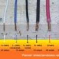 How to choose the right cable cross-section
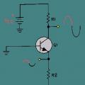 The simplest low-frequency amplifiers using transistors
 Calculation of cable cross-section by power