Laser ironing technology for manufacturing printed circuit boards. Loot technology for manufacturing printed circuit boards. Half and drilling
The need to make hardware periodically arises among many techies. Sometimes the task allows you to screw everything up with wires on the breadboard, and sometimes, unfortunately, you need something more serious. So one day I was overtaken by the need to make printed circuit boards... Laser-ironing technology for handicraft manufacturing of circuit boards is at first very repulsive due to its randomness (what to print on, how to heat it, with what force to press, how to tear it off, etc.), but friends shared their experience , and it turned out that it really isn't that difficult. LUT is undeniably cheaper than any other option, and (surprisingly) quite suitable for two-layer boards.
Those who are interested in something more complex, more expensive and more precise can do it, but our technique (the main element of which is special paper) allows us to consistently work on 0.3/0.3 mm busbars, so in our community there is an opinion that photoresists are not needed.
Anyone who doesn’t see the point in handicraft production of boards will most likely be able to remember a couple of cases when they had to cut tracks and solder wiring on a whole batch of boards. And having made one board at home, you can thoroughly debug it and gain confidence in factory boards.
Below the cut, I will share a deterministic method for manufacturing two-layer printed circuit boards using LUT technology with various backup circuits in case of jambs. From idea to inclusion. We will work with KiCad, Inkscape, sandpaper, iron, ammonium persulfate and engraver.
Any device starts with a circuit. Most board errors can be eliminated at the design stage. And in order for the circuit to be guaranteed to match the board, you need good EDA software. For example, KiCad.
KiCad --> Board
If you are still working with proprietary limited solutions, start with the article or skip this section.
We use the recently released KiCad 5, because I deeply like this program, its community (including CERN) and the idea of multi-platform FOSS in general.
So the algorithm with life hacks:

Board --> SVG
When the board is ready, you need to convert it to SVG for further refinement. It’s better to unload the board from EDA without mirroring, so as not to get confused and mirror it properly.
And we need to mirror it only front layer F.Cu. Since we look at the back layer of B.Cu in the editor from the front, it is already mirrored. For reliability, it is better to place at least some text on both layers and make sure that this text is not readable))
( , ) It is better to upload from KiCad via File | Plot, since it is possible to make all the holes 0.35 mm at once. For manual LUT, greasy holes are not needed, it is better to have more copper and clean it off with a drill.

Actually:
- Load both layers into Inkscape.
- We set the document measurement units to millimeters, and the A4 sheet format.
- Adding even more white lettering to the metallization areas. KiCad can't do this, write in the comments if your EDA can.
- Let's group so that there are only two objects.
- Align (Ctrl+Shift+A), the distance between the layers (their overall holes) should be at least a centimeter.
- We mirror the front layer using the button on the top toolbar.
- Save as SVG.
Now we need to send the SVG to the printer on plain paper. And do the following with this paper:
- Attach components to it and check the footprints (which, in any case, have already come from the store: if you have more than three to five components on the board, it’s difficult to trace everything in one evening)
- Attach to the PCB and punch 4 dimensional holes in the corners that we added
- Take a core (or nail) with a hammer and make a super-precise, shallow dent that will absorb stray drill bits. The impact force must be such as not to deform the board.
- Drill 4 holes with the thinnest drill (0.6-0.8) exactly at 90 degrees. This is perhaps the most difficult part, but mistakes are acceptable; a method for their subsequent correction has been invented.
- If you have a machine, you are lucky.
- If you have a CNC, you are very lucky; figure out all the holes according to the DRL file right now without any cores.
- It is easy to guess that the holes are needed to accurately orient the front layer relative to the back one. If you want something simpler, there is a way without holes: very precisely fold the piece of paper with the template and place the PCB inside. As already mentioned, a slight deviation will not be fatal (unless, of course, the holes have not yet been drilled)
- Another folding modification:
We place freshly printed sheets with the top and bottom layers on top of each other, shining them through with a lamp and aligning them. We fasten in several places along the edges. We put textolite into the resulting envelope.- shared . Thank you!
Ok, this is the section about SVG, and we’ve already moved on to the machines... That’s it, the final touch on SVG and you won’t need a computer anymore:
Fill everything with black so that parts of the PCB that do not belong to the board are not etched and do not saturate the ammonium persulfate with copper. Yes, ferric chloride is also possible, but ammonium is blue.
SVG --> Textolite

Also, we have information about the suitability of paper Black Diamond. Other brands may or may not have the required properties. HP does not fit exactly (melts under the iron), Lomond fits conditionally, "but somehow average". You can experiment with different glossy photo paper for inkjet printing. Write in the comments what it’s like with other papers)
Algorithm:
- Set the iron to heat up to maximum temperature.
- We grind the textolite on both sides with fine sandpaper and a plumbing abrasive sponge (,), dish sponge or an abrasive eraser.
- If your printer can accept formats other than A4, Cut a strip from A4 to the size of the image. Paper is extremely valuable: if you managed to get it, you need to save it.
- We push it into the printer with the narrow side. We check that the image of the two layers of the board does not exceed the width of the cut strip in width and 210 in height.
- We laser print with original toner in a cartridge on this glossy photo paper for inkjet printers.
- Without touching the toner, cut the layers into two separate pieces of paper and make large holes on both layers.
- We insert straight pins (for example, from a PLS/PLD comb) into the 4 dimensional holes.
- Place the front layer.
- We iron it evenly, without pressing too hard, until the paper turns yellow (or any other signs from above, this is still LUT: it’s probably impossible to completely get rid of the magic). The pins can be pulled out when the paper begins to stick and loses its ability to move.
- Without tearing the paper off the PCB, we repeat the last three steps with the back layer.
- Let the textolite cool down: you can put the kettle on to warm up and begin to dissolve the ammonium persulfate.
- Carefully peel off the excess paper from the cooled PCB (without water, this is extremely important). The toner should come off along with the glossy layer of photo paper, that’s how it was intended.


In case of mistakes, you can erase one of the layers with acetone, place the already torn piece of paper on the opposite layer (so that the toner does not come off the board and transfer to the board on which you are ironing) and repeat.
Textolite --> Textolite with tracks
For etching, we need a plastic container (or any non-metallic container in which the board will fit lying down). And also, a disposable spoon or varibashi for stirring the board (against bubbles that interfere with etching).
It is recommended to dilute ammonium persulfate in warm water 1:2. But this is a fairly high concentration, 1:3 or even 1:4 is enough. After all, you can stir it some more later. The recommended temperature for unwinding is 40-50 degrees.
However, keep in mind that overheating all kinds of chemicals is quite dangerous. High concentration, high temperature and copper salts can lead to creepy results.
Technology for manufacturing printed circuit boards at home
"...and experience is the son of difficult mistakes..."
So, the board manufacturing process begins with a schematic diagram of the future device. At this stage, you determine not only how the components will be connected to each other, but also decide which components are suitable for your design. For example: use standard parts or SMD (which, by the way, also come in different sizes). The size of the future board will depend on this.
Next, we decide on the choice of software with which you will draw the future board. While a circuit diagram can be drawn by hand, this cannot be done with a printed circuit board design (especially when it comes to SMD components). I use . I downloaded it a long time ago and have been using it. A very good program, with an intuitive interface, nothing superfluous. In the program we create a drawing of a printed circuit board.
Haven't discovered any secrets yet? So: when the board drawing has already been created, you have made sure that the components are located correctly, you should set the “ground”, i.e. fill the gaps between the tracks and holes; for this purpose, the program has a special function that does this automatically (by default the gap is 0.4 mm). Why is this necessary? So that etching (we'll look at it later) takes less time, it will be easier for you to control the process and it is also useful to do this for circuit design reasons...

Note: When designing a board, try not to make holes smaller than 0.5 mm in diameter, unless, of course, you have a special machine for drilling holes, but more on that later...
Great! We have drawn a drawing of the future printed circuit board, now it needs to be printed on a LASER printer (Lut means laser). To do this, click print. The above-mentioned program creates a special file, in which you can select the number of copies, their location, make a frame, specify the size of the holes and mirror.
Note: if you are making a double-sided printed circuit board, then the front part must be reflected horizontally, and the back part must be left as is. ConcerningSprint- Layout, then it is better to do this at the stage of creating the diagram, and not at the stage of preparing the file for printing, since “glitches” arise with the “mass”, it disappears in some places.
And yet, it is better to print several copies, even if you only need one copy, because defects may appear in the next stages and in order not to run to the printer every time, do this in advance.
What to print on? To begin with, we print it out on a regular sheet of paper to make sure for the last time that everything is done correctly and that all components fit in size. This will also warm up the printer.

Now we set the maximum toner density, disable all saving modes (by the way, it is better to use a fresh cartridge). We take a backing of self-adhesive paper, preferably “velvet” paper (the best result is obtained with it, maybe this is due to the fact that it is thicker), insert it with the shiny side into the printer and press “print”. Ready!

Note: from now on, you cannot touch this paper, only by the edges, otherwise you may stain the drawing!
About reusing the substrate. Let's say that you printed out a drawing, but it only took up half of the sheet, you don't need to throw away the other half, you can print on it too, BUT! for some reason, when printing again, the printer “chews” the paper in 20% of cases, so be careful!
Preparing textolite
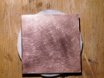
I use regular foil fiberglass laminate 1 mm thick, which is sold in a radio parts store. Since we want to make a double-sided board, we buy double-sided PCB. We cut off the required piece, there is no need to make a reserve, it will not be needed. They cut it off. We take zero sandpaper and sand the textolite until shiny on both sides. If there are small scratches, then it’s okay, the toner will stick better (but without fanaticism!). Next, take acetone (alcohol) and wipe the board on both sides to degrease it. Ready!


Note: when you sand the PCB, pay attention to the corners of the board, very often they are “under-sanded” or, even worse, “over-sanded”, this is when there is no foil left there at all. After wiping with acetone, the board should also not be touched with your hands; you can only grab it by the edges, preferably with tweezers.

Next is the most important stage: transferring the design from paper to textolite. It is done using an iron (lut means iron). Anyone will do here. We heat it to 200 degrees (often this is the maximum temperature of the iron, so we just turn the regulator to maximum and wait for it to heat up).
And now here are the secrets! To transfer a printed circuit board design from paper to PCB, you need to attach the paper to the PCB with the desired side, then press it with an iron and smooth it out thoroughly. Doesn't seem complicated? But the most difficult thing is to apply the iron so as not to sweep away the paper, especially if the scarf is small and you are making it in a single copy; besides, it is not so easy to use the iron. There is an interesting way to make the task easier.
Note: We're looking at making double-sided PCBs, so a little about paper preparation. Some sources advise doing this: transfer one side, seal the opposite side with tape or tape, etch one side, then drill holes, match the pattern of the other side, then transfer it again, seal it, etch. This takes a lot of time because you essentially have to etch two boards! You can speed up the process.
We take two pieces of paper with a design on the front and back sides and combine them. This is best done on a glass window or on a transparent table with lighting. Note! in this case, it is necessary to cut off the pieces of paper with a margin, the more the better, but without fanaticism, 1-1.5 cm is enough. We fasten them with a stapler on 3 sides (no glue!), We get an envelope in which we put the board and let's align it.

The most interesting. We take two pieces of PCB (see the size in the figure), place them with the foil side facing each other, and between them we place an “envelope” with a board, and secure the edges of this sandwich with paper clips so that the PCB sheets do not move relative to each other.

Note: for these purposes, it is better to choose a thinner textolite; it will warm up faster and will be able to deform where necessary.

Now, we take the iron and calmly apply it to our sandwich, and press as hard as we can, first on one side, then turn it over and press on the other. For the best effect, I recommend that after the first pressure, make several circular movements with the iron to be sure that the paper is pressed in all places. You don't need to iron for long, usually no more than 1-3 minutes for everything, but no one will tell you the exact time, because it depends on the size of the board and the amount of toner. The main thing is not to overexpose, because in this case the toner may simply spread, and if you underexpose, the drawing may not be completely transferred. Practice, gentlemen, practice!
Then you can open the sandwich and make sure that the paper is stuck to the PCB on all sides, i.e. no air bubbles. And we quickly carry the board under running water and cool it (with cold water, of course).
Note: If you used a backing from self-adhesive paper, then it will fall off the PCB itself under water and the board will easily fall out of the envelope. If you used a velvet paper backing (thicker), then this will not work with it. We take scissors and cut off the sides of the envelope, then slowly, holding the edge of the paper, remove the paper under running water. As a result, there should be no toner left on the paper; it will all be on the PCB.
At this stage, if defects occur, there are two ways to proceed. If there are too many defects, it is better to take acetone, wash off the toner from the PCB and try again (after first repeating the process of cleaning the PCB with sandpaper).
An example of an irreparable defect (in this case, I started over):


If there are few defects, then you can take a marker for drawing printed circuit boards and fill in the defects.
A good option, there are small holes in the “mass”, but they can be painted over with a marker:


Corrected options. The green shaded areas are clearly visible:


Great, this was the most technologically difficult stage, it will be easier later.
Now you can etch the board, i.e. remove excess foil from the PCB. The essence of etching is this: we place the board in a solution that corrodes the metal, while the metal located under the toner (under the board pattern) remains unharmed, and the one around it is removed.
I'll say a few words about the solution. In my opinion, it is better to poison with ferric chloride, it is not expensive, the solution is very easy to prepare, and overall it gives a good result. The recipe is simple: 1 part ferric chloride, 3 parts water and that’s it! But there are other methods of etching.
Note: you need to add water to the iron, and not vice versa, this is how it should be!
Note: There are two types of ferric chloride (that I have seen): anhydrous and 6-hydrous. Anhydrous, as the name implies, is completely dry, and there is always a lot of dust in the container in which it is sold, this is not a problem. But when water is added, they will actively dissolve, a strong exothermic reaction occurs (the solution heats up), with the release of some kind of gas (most likely it is chlorine or hydrogen chloride, well, it’s a rare dirty trick), which CANNOT BE INHALED, I recommend diluting it in air.
But 6-water iron is already better. This is, in fact, already a solution, water is added, wet lumps are obtained, which also need to be added to the water, but there is no such violent reaction anymore, the solution heats up, but not very quickly and not very strongly, but everything is safe and quiet (windows are still needed open).

Note: the advice that I give here is not the only correct one; on many forums you can meet people who have obtained boards with a different concentration, a different type of ferric chloride, etc. I just tried to summarize the most popular advice and personal experience. So, if these methods did not help, then try another method and you will succeed!
Have you prepared the solution? Great! Select a container. For single-sided ones, this choice is simple, we take a transparent (to see the etching process) plastic box with a lid, put the board on the bottom. But with double-sided boards it's not so simple. It is necessary that the etching speed on each side be approximately the same, otherwise a situation may arise where one side has not yet been etched, but the tracks on the other are already dissolving. To prevent this from happening, you need to place the board vertically in the container (so that it does not lie on the bottom), then the solution around will be homogeneous and the etching rate will be approximately the same. Therefore, it is necessary to take a high capacity so that the board fits “full height”. It is better to choose a narrow transparent jar so that you can observe the etching process.

Next, the solution must be heated (we place it on the battery), this will increase the speed of the reaction, and shake periodically to ensure uniform etching and to avoid the appearance of sediment on the board.
Note: some people put it in the microwave and heat it there, but I don’t recommend you do this, because... I read on one forum that after this you can get poisoned by food from this microwave. There is no direct evidence, but it’s better not to risk it!
Note: to ensure uniform etching, you need to stir the solution (shake the container), but there are more technologically advanced methods. You can attach a bubble generator (from an aquarium) to the container and then the bubbles will mix the solution. I've seen people making oscillating etching pots with a servo motor and a microcontroller that does the "shaking" according to a special algorithm! Here I do not consider each option in detail, because each has its own nuances and the article would then be very long. I described the simplest method, which is perfect for the first boards.
We are waiting, no need to rush!
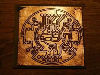
It is very easy to understand that the etching process has ended: there will be no traces of foil between the black toner. When this happens, you can remove the board.
Next, we carry it under water and wash off the remaining solution. Take alcohol or acetone and wash off the toner; there should be foil tracks underneath it. Great, is everything okay? Are there any “under-etched” places? Are there any “over-etched” places anywhere? Great! We can move on!

Note: if defects appear at this stage of production, you are faced with a serious choice: throw away the defect and start over, or try to fix it. It depends on how serious the defects are and how high your demands are on your work.
The next stage is tinning the board. There are two main ways. The first one is the simplest. We take soldering flux (I use LTI-120, but not the one that looks like rosin varnish, which leaves terrible stains on the soldering field, but the alcohol-based one, it is much lighter), generously lubricate the board with it on one side. We take solder and a soldering iron with a wide tip and begin to tin the board, i.e. Cover the entire foil with solder.

Note: do not keep the soldering iron on the tracks for too long, because... Textolite comes in different qualities and some of the tracks fall off very easily, especially thin ones. Be careful!
In this case, solder streaks or unpleasant-looking bumps may appear on the board; it is better to deal with them using a desoldering braid. In those places where it is necessary to remove excess solder, we apply it, all excess solder is removed and a flat surface remains.
Note: you can immediately wrap the braid around the tip and tin with it right away, this may turn out even easier.


The method is good, but to achieve an aesthetically pleasing appearance of the board, some experience and skill is required.
The second method is more complicated. You will need a metal container in which you can boil water. Pour water into a container, add a couple of tablespoons of citric acid and put it on gas, bring to a boil. The solder should not be simple, but one with a low melting point, for example Rose alloy (about 100 degrees Celsius). We throw a few balls to the bottom and see that they have melted. Now we throw the board onto these balls, then take a stick (preferably a wooden one, so as not to burn your hands), wrap it in cotton wool and begin to rub the board, disperse the solder along the tracks, thus achieving an even distribution of solder throughout the board.
The method is quite good, but more expensive, and you need to choose a container, because you will have to use tools in it. It is better to use something with low sides.
Note: you will have to do this operation for quite a long time, so it is better to open the window. With experience you should get faster.
Note: many people do not speak very well of Rose alloy due to its fragility, but it is very suitable for tinning boards using this method.
Note: I myself don’t like this method, because I tried to use it when I made the first board and I remember well how inconvenient it was to “cook” this board in a tin can without tools....Oh, that was terrible! But now...
Both methods have their advantages and disadvantages; the choice depends only on you and your capabilities, desires, and skills.
Note: I further recommend testing the board with a multimeter to make sure that there are no intersections of tracks that should not intersect, that there are no random “nozzles” or any other surprise. If we find a problem, take a soldering iron and remove the excess solder; if that doesn’t help, then use a utility knife and carefully separate the necessary places. This may mean that the board is under-etched in some places, but that's okay.
To do this we use a small drill and a drill bit. Now special drills for printed circuit boards are sold with special sharpening and special grooves on the drill. At first I used a regular drill for metal with a thickness of 0.6 mm, then I switched to a special one and the result was very good. Firstly, even with my budget drill, any PCB can be drilled without any problems, with almost no effort. The drill itself “bites” into it and pulls the tool along with it. Secondly, it leaves a neat entry and exit hole, without burrs, unlike a standard drill, which literally “tears” the PCB. Thirdly, this drill almost does not slip, i.e. You just need to get to the right place the first time and it won’t go anywhere. A miracle, not a tool! But it also costs a little more than a regular drill.
Note: to “get to the right place right away” it is better to use an awl or a special tool for punching, just do not make too deep cuts, this may direct the drill in the wrong direction. Also: this drill has one drawback - it breaks easily, so it is better to use a special machine to drill holes or hold the drill strictly vertically. Believe me, it breaks very easily! Especially when you need to drill a hole of 0.3 mm or 0.2 mm, but this is already jewelry work.
Ready! That's all! We solder the through holes with thin wires and we get neat hemispheres on the board, it looks very nice. Now you just need to solder all the components of the circuit and make sure that it works, but this is a topic for another article. And here's what I got:


That's all. Once again I want to emphasize that here I only tried to summarize all the materials that I managed to find about LUT, and my experience. It turned out a little long, but in every case there are many nuances that must be taken into account to achieve the best result. The last piece of advice I can give you is: you need to try, try to make boards, because mastery comes with experience. And at the end I will once again quote the epigraph: “...and experience is the son of difficult MISTAKES...”
If you have any questions, you can leave them in the comments. I will also be grateful for constructive criticism.
When a laser printer is available, radio amateurs use a printed circuit board manufacturing technology called LUT. However, such a device is not available in every home, since even in our time it is quite expensive. There is also a manufacturing technology using photoresist film. However, to work with it you also need a printer, but an inkjet one. It’s already simpler, but the film itself is quite expensive, and at first it’s better for a novice radio amateur to spend the available funds on a good soldering station and other accessories.
Is it possible to make a printed circuit board of acceptable quality at home without a printer? Yes. Can. Moreover, if everything is done as described in the material, you will need very little money and time, and the quality will be at a very high level. In any case, the electric current will “run” along such paths with great pleasure.
List of necessary tools and consumables
You should start by preparing the tools, devices and consumables that you simply cannot do without. To implement the most budget-friendly method for manufacturing printed circuit boards at home, you will need the following:- Software for drawing design.
- Transparent polyethylene film.
- Narrow tape.
- Marker.
- Foil fiberglass.
- Sandpaper.
- Alcohol.
- Unnecessary toothbrush.
- Tool for drilling holes with a diameter of 0.7 to 1.2 mm.
- Ferric chloride.
- Plastic container for etching.
- Brush for painting with paints.
- Soldering iron.
- Solder.
- Liquid flux.
There are a huge number of programs for developing printed circuit boards today, but for a novice radio amateur, the simplest option would be Sprint Layout. The interface is easy to master, it is free to use, and there is a huge library of common radio components.
Polyethylene is needed to transfer the pattern from the monitor. It is better to take a stiffer film, for example, from old covers for school books. Any tape will be suitable for attaching it to the monitor. It’s better to take a narrow one - it will be easier to peel off (this procedure does not harm the monitor).
It’s worth looking at markers in more detail, as this is a sore subject. In principle, any option is suitable for transferring a design onto polyethylene. But to draw on foil fiberglass, you need a special marker. But there is a little trick to save money and not buy quite expensive “special” markers for drawing printed circuit boards. The fact is that these products are absolutely no different in their properties from ordinary permanent markers, which are sold 5-6 times cheaper in any office supply store. But the marker must have the inscription “Permanent”. Otherwise nothing will work.

You can take any foiled fiberglass laminate. It's better if it's thicker. For beginners, working with such material is much easier. To clean it, you will need sandpaper with a grit size of about 1000 units, as well as alcohol (available at any pharmacy). The last consumable can be replaced with nail polish mixing liquid, which is available in any house where a woman lives. However, this product smells quite nasty and takes a long time to dissipate.
To drill the board, it is better to have a special mini-drill or engraver. However, you can go a cheaper route. It is enough to buy a collet or jaw chuck for small drills and adapt it to a regular household drill.
Ferric chloride can be replaced with other chemicals, including those you probably already have in your home. For example, a solution of citric acid in hydrogen peroxide is suitable. Information on how alternative compositions to ferric chloride are prepared for etching boards can be easily found on the Internet. The only thing worth paying attention to is the container for such chemicals - it should be plastic, acrylic, glass, but not metal.
There is no need to talk in more detail about the soldering iron, solder and liquid flux. If a radio amateur has come to the question of making a printed circuit board, then he is probably already familiar with these things.
Development and transfer of a board design to a template
When all of the above tools, devices and consumables are prepared, you can begin developing the board. If the device being manufactured is not unique, then it will be much easier to download its design from the Internet. Even a regular drawing in JPEG format will do.
If you want to go a more complicated route, draw the board yourself. This option is often unavoidable, for example, in situations where you do not have exactly the same radio components that are needed to assemble the original board. Accordingly, when replacing components with analogues, you have to allocate space for them on fiberglass, adjust holes and tracks. If the project is unique, then the board will have to be developed from scratch. This is what the above-mentioned software is needed for.
When the board layout is ready, all that remains is to transfer it to a transparent template. The polyethylene is fixed directly to the monitor using tape. Next, we simply translate the existing pattern - tracks, contact patches, and so on. For these purposes, it is best to use the same permanent marker. It does not wear off, does not smudge, and is clearly visible.
Preparation of foil fiberglass laminate
The next step is the preparation of fiberglass laminate. First you need to cut it to the size of the future board. It is better to do this with a small margin. To cut foil fiberglass laminate, you can use one of several methods.Firstly, the material can be cut perfectly using a hacksaw. Secondly, if you have an engraver with cutting wheels, it will be convenient to use it. Thirdly, fiberglass can be cut to size using a utility knife. The principle of cutting is the same as when working with a glass cutter - a cutting line is applied in several passes, then the material is simply broken off.


Now it is imperative to clean the copper layer of fiberglass from the protective coating and oxide. There is no better way than sandpaper to solve this problem. The grain size is taken from 1000 to 1500 units. The goal is to obtain a clean, shiny surface. It is not worth sanding the copper layer to a mirror shine, since small scratches from sandpaper increase the adhesion of the surface, which will be needed later.
Finally, all that remains is to clean the foil from dust and fingerprints. To do this, use alcohol or acetone (nail polish remover). After processing, we do not touch the copper surface with our hands. For subsequent manipulations, we grab the fiberglass by the edges.
Combination of template and fiberglass

Now our task is to combine the pattern obtained on polyethylene with the prepared fiberglass laminate. To do this, the film is applied to the desired location and positioned. The remains are wrapped on the reverse side and secured with the same tape.


Drilling holes
Before drilling, it is recommended to secure the fiberglass laminate with the template to the surface in some way. This will allow for greater accuracy and will also prevent sudden rotation of the material as the drill passes through. If you have a drilling machine for such work, then the problem described will not arise at all.
You can drill holes in fiberglass at any speed. Some work at low speeds, others at high speeds. Experience shows that the drills themselves last much longer if operated at low speeds. This makes them more difficult to break, bend and damage the sharpening.
The holes are drilled directly through the polyethylene. Future contact patches drawn on the template will serve as reference points. If the project requires it, we promptly change drills to the required diameter.
Drawing tracks
Next, the template is removed, but not thrown away. We still try not to touch the copper coating with our hands. To draw paths we use a marker, always permanent. It is clearly visible from the trail it leaves. It is better to draw in one pass, since after the varnish, which is included in the permanent marker, has hardened, it will be very difficult to make edits.
We use the same polyethylene template as a guide. You can also draw in front of the computer, checking the original layout, where there are markings and other notes. If possible, it is better to use several markers with tips of different thicknesses. This will allow you to draw both thin paths and extensive polygons more efficiently.


After applying the drawing, be sure to wait some time necessary for the final hardening of the varnish. You can even dry it with a hairdryer. The quality of future tracks will depend on this.

Etching and cleaning marker tracks
Now comes the fun part - etching the board. There are several nuances here that few people mention, but they significantly affect the quality of the result. First of all, prepare the ferric chloride solution according to the recommendations on the package. Usually the powder is diluted with water in a ratio of 1:3. And here's the first piece of advice. Make the solution more saturated. This will help speed up the process, and the drawn paths will not fall off before everything necessary is etched out.
Immediately the second tip. It is recommended to immerse the bath with the solution in hot water. You can heat it in a metal bowl. Increasing the temperature, as has been known since school, significantly accelerates the chemical reaction, which is what etching our board is. Reducing the procedure time is to our advantage. The tracks made with a marker are quite unstable, and the less they sour in the liquid, the better. If at room temperature the board is etched in ferric chloride for about an hour, then in warm water this process is reduced to 10 minutes.
In conclusion, one more piece of advice. During the etching process, although it is already accelerated due to heating, it is recommended to constantly move the board, as well as clean off the reaction products with a drawing brush. By combining all the manipulations described above, it is quite possible to etch out excess copper in just 5-7 minutes, which is simply an excellent result for this technology.

At the end of the procedure, the board must be thoroughly rinsed under running water. Then we dry it. All that remains is to wash away the traces of the marker that are still covering our paths and patches. This is done with the same alcohol or acetone.

Tinning of printed circuit boards
Before tinning, be sure to go over the copper layer again with sandpaper. But now we do it extremely carefully so as not to damage the tracks. The simplest and most accessible method of tinning is the traditional one, using a soldering iron, flux and solder. Rose or Wood alloys can also be used. There is also so-called liquid tin on the market, which can greatly simplify the task.But all these new technologies require additional costs and some experience, so the classic tinning method is also suitable for the first time. Liquid flux is applied to the cleaned tracks. Next, solder is collected onto the soldering iron tip and distributed over the copper remaining after etching. It is important to warm up the traces here, otherwise the solder may not “stick”.

If you still have Rose or Wood alloys, then they can be used outside the technology. They melt just fine with a soldering iron, are easily distributed along the tracks, and do not bunch up into lumps, which will only be a plus for a beginning radio amateur.
Conclusion
As can be seen from the above, the budget technology for manufacturing printed circuit boards at home is truly accessible and inexpensive. You don't need a printer, an iron, or expensive photoresist film. Using all the tips described above, you can easily make the simplest electronic radios without investing a lot of money in it, which is very important in the first stages of amateur radio.
This video lesson shows the implementation of LUT technology, which is used to make a double-sided printed circuit board. At home you can make compact ones using SMD elements. Here, using the example of a charger for a 18650 lithium-ion battery taken from an old laptop battery, we will go through the process of creating a board from printing a drawing to turning it on.
Watch the compressedvideo channel video
First of all, we draw a printed circuit board in the Eagle program for its subsequent manufacturing using laser-iron technology. About high-power lasers. The program is free for one- and two-sided applications. We upload each side of the signet in black and white into a graphic editor and combine them to print on one sheet. We will print on tracing paper. But to prevent the printer from jamming it, you will need glue and an A4 sheet. We buy 40 sheets of tracing paper at the nearest stationery store.
First, look for the smooth side. We take out a sheet of paper and check where it slides more than usual, this is the top side. Now we bend the sheet of paper so that we can insert tracing paper. 1-1.5 cm is enough. We do not coat it too much with glue, as it will go inside the printer, and we glue the tracing paper evenly. If you make it crooked, the two sides won't match.
Preparing a “sandwich”. Now we fold the sheet at the top to place it in a manual feed printer. Insert with tracing paper facing up. We get a fingerprint. We cut out a large piece and fold it along the fold, aligning the two sides of the board to the light. Tracing paper is ideal for this. All holes are visible and can be accurately aligned. We glue the sheet together to make a pocket, and we will place the board in it. To do this, coat it with glue on both sides.
Preparing a board for implementing LUT technology
To prepare the board we will need cleaning powder. If it says it cleans copper, that's it. You can take another one, or even paste. GOI (but not sandpaper). We take the powder and begin to clean the board until it reaches a mirror shine. Once there are no dark spots left on the board, it can be placed in the pocket. Once cleaned, you can only pick it up by the edges so as not to leave greasy fingerprints.
We place the board in the finished pocket and align it so that the entire print falls on it. Everything is ready for ironing. It is better to take a simple one without steam. Temperature at maximum. We carefully begin to iron over the entire area. The tracing paper sticks to the board and you can clearly see how the toner darkens. You don’t have to press too hard, but you need to iron both sides. Gradually the toner darkens and begins to bleed through the tracing paper. Once this has happened, everything is ready for the next operation. It is important not to overdo it, because the toner may spread and bottlenecks between the tracks may be flooded and will have to be cleaned up.
Now the tracing paper needs to be washed off. The toner will remain on the board, the paper will gradually come off. We cut it so that it all fits in the bath. We take ordinary water and throw the board there. We wait until it gets wet. After some time, the tracing paper begins to bubble and can be carefully removed. When wet, it comes off the board easily. The toner remains, covering all areas that we need to leave unetched. The tracing paper curls into lumps and gets wet. As a result, we get a beautiful, almost factory board.
It looks like it’s ready, but let’s take a magnifying glass and check how it turned out. It is clearly visible that there are pieces of paper left. The board will not be etched in these places. You need to remove the paper between the tracks. To do this, use a bristle brush. Moving along the paths, so as not to damage them, remove the remaining paper. When the board is dry, the places where the tracing paper remains are clearly visible, but this is not critical here. We drill a couple of holes on the side to insert the wire. She will help hold the board while we poison. We use ammonium persulfate. This is a rather aggressive substance and it is not recommended to dip your fingers in it. We take hot water from the tap. We dose it like this: one tablespoon of water per one teaspoon without a slide of persulfate. 5 spoons are enough for such a board. A water bath is also needed, since the etching reaction actively cools the solution.
Stir with a plastic or glass rod. And remember that if the solution gets on your clothes, it will leave holes. Place the board in the solution and stir for about five minutes. At first the solution is transparent, then gradually turns blue. This copper goes into solution in the form of copper sulfate. We see that the copper has brightened. There is very little left until it completely disappears. The layer is very thin and it will disappear now.
After about five minutes, the board is cleaned, there are small spots left that need to be cleaned with a brush to speed up the process. Using a soft brush, remove any remaining copper.

The metal tip is wrapped with electrical tape to prevent it from being etched. We take white spirit, which dissolves printer toner well. We need to clean the board to prepare it for tinning. You can also clean with acetone or use nail polish remover. After washing off the toner, the resulting product shines with copper traces.
Tinning
We will tin with Rose alloy. To do this, we need a ladle, which will be damaged and no longer suitable for anything. A little citric acid, gloves, tweezers and the alloy itself. Rose has a melting point of just under 100 degrees. It consists of small granules, one of which is enough to tinning a board. Add a spoonful of citric acid and a few tablespoons of salt. And we boil it. We throw a grain of alloy onto the board.
Rose, if the temperature is sufficient, will melt. We try to smear it with a cotton swab. If it doesn’t melt, then you need to add more salt to raise the boiling point. The alloy should spread easily and effortlessly into a thin layer. We spread the alloy without lumps so that SMD elements can easily become. Now, within the framework of LUT technology, you can proceed to the next stage.
Drilling the board
Let's start drilling. A high-speed mini drill with a collet clamp was used. It allows you to clamp drills without distortion. Drills with a thicker shank are better. Drills of two sizes 0.5 and 0.8 are used; they can be taken for one size of collet clamp. It is better if you use a machine, but you can also carefully drill with a drill, it must be held strictly vertically. Then the holes on the top and bottom sides will fit exactly into the track seats. After drilling, you can make sure that both sides match perfectly.
Cutting the board
Now you can use regular metal scissors to cut the board to size. This can only be done if it is thin enough. The board is ready for soldering. To solder SMD elements, you need a special paste SOLDER PASTE, W001 is used, which is usually sold in tubes. Don't forget to store it in the refrigerator. We carry out soldering with a soldering hair dryer. Apply a drop of solder paste to each soldering point. Just a little bit is needed. If you don't have a needle, you can do this with a regular toothpick. A small drop is enough for soldering; if there are too many, you can end up shorting adjacent tracks. 
Parts distribution
We put the details in place. You can arrange them roughly, but make sure they stay on the paste. When soldering, they are aligned using surface tension forces. Particular attention should be paid to microcircuits - they need to be placed more precisely. They, of course, also level out. But if they are placed crookedly, then you can get a short circuit in the tracks and either resolder them or remove the resulting “snot” with a soldering iron.
For our paste, a temperature of 230 degrees is enough; we set the minimum airflow so as not to blow our parts off the board. Heat each part until the solder melts. We see that the parts are aligned in place. Soldering with a hairdryer is a pleasure. It takes a long time to prepare, but the soldering itself is quick and high quality. In this case, you can solder the entire side of the board at a time. As a result, it turns out much faster than with a soldering iron.
Now the hardest part, three output parts that also need to be soldered, the rest are already in place. Before soldering the LEDs, it is a good idea to check their polarity. We switch the tester to the diode testing mode and, by the glow of the LED, determine where the plus and minus are. Let's take a tuning resistor, install it in place and solder it using a soldering iron. Since the board is double-sided, it is necessary to solder on both sides. The pins of the parts were also used to transmit a signal between the parties.
For convenience, it is better to use a “third hand” card holder, but you can do it without it, although it is less convenient. The result is this board for charging the battery, made using LUT technology. It is double-sided, there are both SMD and lead parts. Just look how convenient this thing is.
http//journal.caseclub.ru
So many articles have already been written about laser ironing technology (LUT) on the Internet that there is little point in coming up with your own - everything has long been told, shown and done. And for those who don't like to read (oh brave new world!), hundreds of videos have been made. However!..
As always, allow the unfinished lecturer in me to start from afar. What is printed circuit board? This, as Tamara Antonovna taught us, is a dielectric base on which printed conductors are applied and mounted elements are installed, connected to each other by soldering or gluing according to the electrical circuit diagram. It looks something like this:

Here the dielectric base is made of fiberglass, and copper printed conductors run along only one side of it. There are also double-sided boards, and there are multilayer ones, in which the tracks also pass inside boards, but for simple circuits, the example of which I will use to talk about LUT, a classic single-sided printed circuit board is absolutely suitable.
General principle of creating a printed circuit board

1. The base material is foil dielectric (getinax, textolite, fiberglass).

2. Installed on foil photo template- a device that carries information about the pattern of printed conductors. Its main task is to protect copper from destruction in the right places (purple stripes) and leave open areas that need to be removed (blue stripes).

3. Some photo masks are designed in such a way that after installation they do not require any additional actions. For example, if the drawing of the conductors was done by hand with nail polish or a particularly tenacious marker. Photoresist requires exposure and washing, paper for LUT... However, it will come to that. The main thing is that it is now applied to the foil mask, which follows the contours of tracks and contact pads and protects them from destruction in the etching solution.

4. The workpiece is immersed in the solution, where the unprotected areas of the foil dissolve. Copper feels great under a mask.

5. Workpiece after etching. Nothing superfluous, just printed conductors and contact pads, still securely covered with a mask.

6. The mask is removed, and the conductor pattern shines with copper.

7. Then connecting holes are drilled, which pass through the contact pads, or “spots”.

8. And finally, the hanging elements are installed.
Now I propose to move from theory to practice, following a simple plan:
1. Making a photo mask
2. Transferring the design to the workpiece
3. Etching
4. Drilling connection holes
5. Assembly
1. Making a photo mask
The pattern of printed conductors can be obtained in different ways: lay out the board yourself, download the required “signature” on the Internet, redraw it from the “Radio” magazine for 1988... I chose the program Sprint Layout.

What's the point of telling how to use it if there are plenty of video tutorials and articles for it? My experience working with P-CAD And Altium Designer, and many things are done by analogy with sPlan.


It is more convenient to draw a board as if you were looking at its elements from above. Then the first leg of the microcircuit is on the top left, and KT315 The emitter-collector-base are in their usual places. The board itself is considered transparent, like glass (a visual aid to help), so the inscriptions made in copper must be mirrored.


On the left is the board during design (the text is mirrored), on the right is a preview of this fragment from the foil side (the text is readable normally).

I usually send two copies of the board for printing - it doesn’t always work out well the first time. Of all the layers to be printed, you only need to leave M2 And P, if the outline of the board is drawn in it (I used to like to draw it on M2). Right now, those who like to draw boards from the side of the tracks, in which the numbering of microcircuits starts from the top right, and the text is initially readable, put a tick in front of the “Mirror” option.
You need to print, of course, on laser printer, disabling all possible toner saving modes in its settings. Almost all existing guide articles insist on using old printer™, which spits on nature and prints in a thick layer. Exact printer models (or at least the last year of production suitable™), alas, these articles are not named.

to my HP M1120 LaserJet MFP eight full years, which makes it old enough™, but still suitable for LUT.
N.B.! It is advisable to perform wide conductors and other relatively large areas of copper with a “polygon” tool filled with a 0.3...0.5 mm mesh. The printer may not be able to press the toner evenly over a large area (especially if the cartridge is old), which will lead to defects in the continuous pattern. Filling with a mesh allows you to get around this limitation.
As for paper, you will most likely have to experiment. There is special paper for LUT on Aliexpress, there is wax paper, there is photo paper; someone uses tracing paper or backings from self-adhesive paper. For me, the “it” is thin, slightly glossy paper from magazines. It is thin, that is, the inner sheets. The thick, completely glossy covers didn't do it justice.
However, do not rush to quietly take magazines away from your favorite doctor’s waiting room - most likely, they are so tattered that no toner will stick to them. Look for something that you almost never picked up. Reader Anton suggests using advertising or party leaflets.


After the drawing is printed, you can cut it out and name it disposable photomask and proceed to the next stage.
Update from 06/16/19
2. Transferring the design to the workpiece


To obtain a high-quality pattern of printed conductors, it is necessary to clean the workpiece from oxides, sweat and grease traces and other contaminants. To do this, the surface of the foil is sanded using P600 grit sandpaper in a circular motion.

After this, the workpiece is cleaned of abrasive dust and degreased, for example, with isopropyl alcohol.


A photomask (or several at once) is applied to the surface of the foil, then the blank is enclosed in an “envelope” of a pair of folded ones in half or three clean sheets of paper. Under the “envelope” there is a stack of another ten sheets of paper - used ones are allowed here.


After this, use an iron turned on at maximum power to evenly heat the workpiece and, without pressing too hard, iron it for 2...5 minutes (depending on the size of the board). The toner, softening under the influence of heat, loses adhesion to glossy paper and transfers to the surface of the foil.


The “envelope” turned yellow after heating. The workpiece must be allowed to rest so that it cools down to a temperature where it is just becoming possible to hold it in your hands.

After this, it is lowered into a cuvette with warm water, and after waiting 5...10 minutes, the paper begins to peel off.


Its outer layer can be easily removed with tweezers; deeper layers require rolling with your fingers. Correctly transferred toner onto foil is not easy to scratch with a fingernail, so you can roll up the paper without fear. If the tracks are not imprinted on the foil or come off along with the paper, it means that the transfer technology has been broken in some way. Most often, this indicates insufficient warm-up time or its unevenness. Sometimes it’s a matter of poor choice of paper or poorly cleaned PCB.

Small fragments of paper remaining inside the “spots” and between the contact pads can be conveniently removed with a bayonet-shaped probe.


As a result, a mask should remain on the surface of the foil, repeating the pattern of the conductors, but now in a mirror image in relation to the project.
There were some defects - and if in the large board only the wide ground path was damaged, then in the small one several “spots” were hesitantly printed. Local underheating as it is.

After drying, the mask takes on this appearance. Now is the time to spin it at different angles to maybe see a glimpse of copper in the middle of some track.


An example of another board shows an isolated “patch” and a thin crack on the track next to it.


Textolite cuts perfectly excellent metal scissors. You can’t do anything good with a bad tool, as my reader Maxim says, so two boards with crushed edges came out from under the shitty scissors. I temporarily put the large one aside, but the small one had to be sent for rework.

The toner washes off well with acetone, but it is difficult to get it in its pure form, and there is no particular need for it. Nail polish remover copes with this task. Having read the composition, you can see that, in addition to the useless chamomile extract, there is the desired acetone.


The process is not entirely beneficial for the lungs, so it is better to do it with the window open.

The second transfer of the drawing turned out to be more successful.

Inside the bottom stack of paper, meanwhile, its own laser-iron technology takes place.


If necessary, the drawing is retouched, if it does not correspond to the original - for this, acrylic paints or nail polish are used.

I know for sure, Where take good metal scissors, I just don’t know When you can take them. And innate greed does not want to give up even such a narrow strip of copper to the etching solution. So I sealed it with tape.
3. Etching
There are different recipes for etching solutions, but the most suitable for the “knee laboratory” is hydrogen peroxide and citric acid. Unlike the ferric chloride solution popular among “old school” radio amateurs, you don’t have to go to special stores to get the ingredients for this holiday. Peroxide can be bought at the pharmacy, citric acid - at the grocery store, salt - found in the kitchen.

Despite all the numbers that adorn articles about LUT, I don’t think any of their authors weighed 10 grams of citric acid and measured out 50 ml of peroxide. Most likely, everyone is quietly pouring peroxide so that it covers the board, and pouring out a handful of acid - the same quantum satis.

Not forgetting, of course, to salt the solution.

Plastic holders made from waste, glued to the PCB with hot-melt adhesive, will help you twist the workpieces without the need to dip your fingers into the solution.

IN plastic Hydrogen peroxide is poured into the cuvette and citric acid and salt are added, thoroughly stirring the mixture until they are completely dissolved. The glass rod from the “Young Chemist” set is very convenient in this aspect. After this, the workpieces are immersed in the solution.


Small bubbles in the solution and pinking of the copper are a sign that you are on the right path, comrades!


Etching occurs at room temperature, but to speed it up, you can heat the solution in a water bath. The process takes 5...20 minutes (depending on the size of the workpiece and the amount of copper removed). The solution must be constantly stirred and large air bubbles removed from it - to do this, just shake the workpieces themselves using the thoughtfully made holders.

As the solution becomes saturated with copper, the etching rate decreases (this can be seen by a decrease in the number of bubbles and the solution turning turquoise). In this case, it is advisable to replace the solution, although it is permissible to add peroxide and add acid and salt.

After etching, the workpieces are thoroughly washed to remove any remaining etchant. The used solution can be poured into the sink - unlike ferric chloride, it does not leave any stains.
N.B.! The solution is prepared as needed and cannot be stored, since hydrogen peroxide tends to spontaneously decompose. Considering the amazing simplicity of the recipe, as well as the availability and low cost of the components, this can hardly be considered a disadvantage.


The protective mask made of toner and acrylic paint is washed off with the same “Marigold”.


The extended paths were made with fine mordants. Apparently two layers of paint weren't enough.
4. Drilling connection holes
From a manufacturability point of view, it is advisable that as many holes as possible be made with the same diameter. IN Sprint Layout You need to keep an eye on this, especially if you use other people's macros. There are two most common hole diameters: 0.8 mm (resistors, capacitors, DIP chips, small diodes and transistors) and 1.0 mm ( L78XX, 1N4007, KT815, MLT-1).

The centers of the holes are marked with an awl.
 Loot PCB manufacturing technology
 Chinese electric lighter circuit Thyristor pcr 406 domestic analogue
 How to make a DNA model from ordinary materials